Introduction
If you’ve ever used an (FPGA) development board or other electronics with USB (keyboard, 3d printer, …), there’s a good chance that you’ve used an USB bridge chip, colloqually called “FTDI chip”, even though nowadays there’s many clones and similar chips not from the original manufacturer. The most famous FTDI chips are the USB<->JTAG/I2C/UART bridges used to enable microcontrollers or FPGAs without native USB to be JTAG-programmed and debugged via USB and for establishing a virtual serial port between a computer and microcontroller’s UART via USB.
But that’s old news - USB 3 has been here for a long time and so have FTDI’s USB 3 bridge chips FT600 and FT601. They provide a high-bandwidth interface between PC and PCB. I’ve used them in different projects where a high speed link between FPGA and PC was needed - most recently in a custom SDR project to transfer sample data to the PC. In this project, I’m using one of the cheapest FPGAs on Mouser (10 €) together with an FT601Q (8.50 €) to transfer just above 3 Gbps of net data to the PC.
Misconceptions
Because of the wide adaption of the USB 2 bridge chips, there are some common misconceptions about the USB 3 chips which do have quite different use cases:
- They don’t provide JTAG / I²C / UART. FT600 and FT601 are pure data movers and only provide a custom parallel bus interface of 16 bit (FT600) or 32 bit (FT601).
- There’s no “virtual COM port” on the PC side. Although they just do data transfer, the FT60X aren’t “fast COM ports” - this means we’ll have to take care of lower level concerns like preparing buffers and individual transfers ourselves (-> ).
Pro’s and Con’s

Different from the FT2xx chips, the USB 3 chips don’t get too much love online, see reddit, and this and this forum posts. So let’s make this quick, yes the interface is clunky and timing can be a bit tricky (see below). But…
- If you are running a data heavy application streaming large chunks of data (as opposed to frequent back and forth of short messages), the interface’s quirks can be designed away quite well.
- It’s not even half the price of Infineon’s FX3, which is great but also more work to setup.
- PCB design is easy and the PHY seems to be quite robust. On my SDR PCB, it’s working with half the recommended decoupling caps assembled and achieves full throughput via 50 cm of cable into an USB 3 Hub + another 2 meters of cable to my PC.
Interface quirks

Transactions in both directions are always initiated by the USB host (i.e. computer with relevant driver). The “FIFO master” can’t write to the FIFO even if there is space, if a read transaction has not been initiated by the PC before. And it can’t write any more data than was requested by the PC.
The FT60x also drives two relevant control signals, RXF_N and TXE_N. If you’ve ever come close to a FIFO before, you’re probably wondering why a full signal is emitted for the RX side and an empty signal for the TX side. Typically, when writing to a FIFO (TX), you’re more interested in knowing whether there is some space left to write to (not full) instead of whether all of the space is available (empty). And vice versa for the RX side. Luckily, this is actually what those pins do and they are just named wrong. Still makes you wonder how you can make a chip that literally has “FIFO” in the name and then fumble the naming of two important FIFO control signals 🤔.
RXF_N is actually “RX FIFO empty”. TXE_N is actually “TX FIFO full”.
Pipe abort procedure
The nature of the interface (i.e. you have two kind-of-masters) can make it difficult to recover from an unknown state. If you’re using this chip in a serious product you should take a look at the comically complicated “abort recovery procedure” in this app note.
Timing
There are two aspects to timing closure which can both be tricky in this instance. Both are related to each other but we can make our lives easier by seperating them out:
- I/O delay timing, i.e. setup and hold of data and control signals between the chips
- Empty/full and read/write handshake, i.e. reacting to FIFO state changes

I/O constraints (set_input_delay, set_output_delay) are often considered tricky and lead to confusion as exemplified in the posts linked above. In my opinion, even the constraints in the official app note are wrong, which would certainly explain some of the frustration out there.
This confusion can stem from thinking about I/O constraints as describing some combination of delays in the input / output path of the FPGA and PCB. While this isn’t wrong, it’s only half of the story because such delays have to be expressed relative to some clock edge - and sometimes the edges are easily mixed up. To avoid this, we can think of I/O delays as another parameter in our normal setup and hold checks - where launch edge and capture edge are clearly defined anyways. If we then think about the relevant delays for the worst case setup and hold checks in both input and output direction, we arrive at the four delay values and respective capture edges to specify the constraints.
The timing arrows in the datasheet timing diagram are given in the form of “setup and hold” times relative to the capture edge. This makes sense when specifying requirements at the chip’s input flops. It makes less sense for the “Output Data” direction because the actual, physical delay times related to the output data are a product of the launch edge and some clock-to-q delay (and potential phase shift and additional delays). The conversion is trivial but clock frequency dependent. Therefore, in a datasheet it would have been advantageous to specify the output delays relative to the launch edge, keeping the whole diagram frequency independent.
Draw a timing diagram with two data cycles and your target clock period because it forces you to think about launch and capture edges.

SDC
See below for the explanation of how to derive these.
Delay constraints used in setup analysis are specified with -max, as in maximum / late analysis. Delays used in hold analysis are specified with -min, as in minimum / early analysis.
If your traces are approximately length matched, you can just set $t_\mathrm{mismatch,max}$ to a small positive and $t_\mathrm{mismatch,min}$ to a small negative safety margin, like $\pm 0.2 \mathrm{ns}$. If you have serious trouble meeting timing, you can also specify individual trace delays for each data pin instead of using the min/max approximation.
|
|

Verifying
Sometimes it’s easy to flip a sign here and there when writing constraints and so I recommend to generate four timing reports and check whether the delays are factored in with the correct sign:
|
|
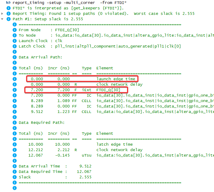
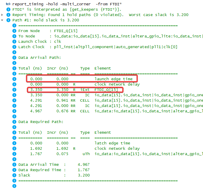
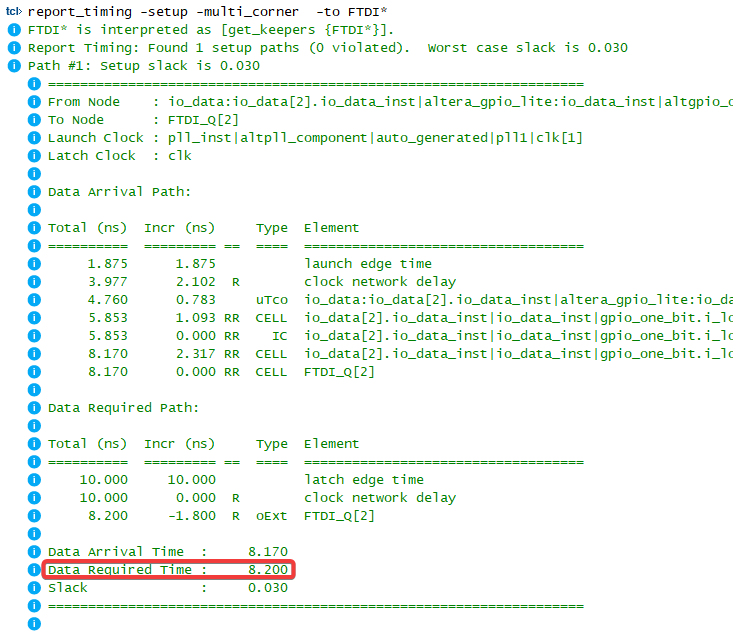
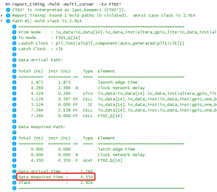
I’m using a phase shifted clock (->Tips) to drive the output registers and Intel Quartus incorporates this in the timing report by shifting the “launch edge time”, which is what can be seen in the two output reports. Vivado would likely factor in a phase shift as a latency in the clock path.
Explanation
Starting with the “to FPGA” direction (i.e. set_input_delay), for the setup check at the FIFO master’s input, we’re interested in the latest arrival of the data versus the clock. The first component of that delay is propagation delay from FT60X to the FPGA. Since both clock and data originate from the FT60X, we only have to consider the difference in trace delay. The second component is the maximum clock-to-q delay at the FTDI’s output which we can derive to be around 7 ns as shown.
For the hold check, we care about the earliest point after a launch edge, at which the data may start to change. There’s a small gotcha here because the earliest point at which the data may start changing is actually at the end of the green section in the diagram because the green section signifies stable data. The minimum clock-to-q delay is T2 in the original diagram.
$$ \begin{align*} t_\mathrm{input,min} &= t_\mathrm{trace,data,min} - t_\mathrm{trace,clk} &+ t_\mathrm{CQ,min} \\ &= t_\mathrm{mismatch,min} &+ 3.5 \mathrm{ns} \end{align*} $$For the “from FPGA” direction (i.e. set_output_delay), we have to consider an additional complication because here, the clock originates from the FT60X and data from the FPGA (not source synchronous). This means that not only the trace delay mismatch (which can be kept relatively small even for long traces) but also the absolute trace delay comes into the equation. Specifically, the clock delay $t_\mathrm{trace,clk}$ occurs on the way from the FT60X to the FPGA and then on the way back, an additional $t_\mathrm{trace,data}$ happens.
The setup check is concerned with the latest arrival of data relative to the earliest sampling time at the receiver. The earliest sampling at the receiver can be understood to be happening one setup time before the clock edge. While the setup time $t_\mathrm{su} = T3$ isn’t a delay but a property of the receiver, it makes sense that we need a way to factor it into our setup check because the timing engine for our FPGA has no way of knowing about it inherently.
$$ \begin{align*} t_\mathrm{output,max} &= t_\mathrm{trace,data,max} + t_\mathrm{trace,clk} &+ T3 \\ &= t_\mathrm{trace,data,max} + t_\mathrm{trace,clk} &+ 1 \mathrm{ns} \end{align*} $$The hold check is actually benefitted by the addition of the absolute trace delays. This is because both the clock and data delays contribute to the data at the receiver to arrive later. The hold time $t_\mathrm{h} = T4$ is factored in with negative sign (see below).
$$ \begin{align*} t_\mathrm{output,min} &= t_\mathrm{trace,data,min} + t_\mathrm{trace,clk} &- T3 \\ &= t_\mathrm{trace,data,min} + t_\mathrm{trace,clk} &- 4.8 \mathrm{ns} \end{align*} $$Tips
Phase shifted output clock
At certain trace lengths, it will be impossible to meet timing without introducing additional delays into the clock or data path. An easy way to do this is using a PLL/DLL to phase-shift the incoming clock and use that phase-shifted version to drive the output flip-flops. If timing becomes difficult between the internal logic and the output flip-flops, another set of flip-flops driven by the non phase-shifted clock can be introduced before the output flip flops.
Tristate drivers
If the output timing is failing, the cause can be the path through the output enable of the tristate output drivers. This is because switching an IO buffer from output to input or vice versa is often much slower than driving a change to the output signal. In the case of the FT60X, we are ideally reading and writing larger chunks of data (e.g. 1024 byte packets) such that the bus turnaround does not happen too often. In that case, timing can be relaxed using set_multicycle_path (see SDC above) to allow the tristate drivers an additional cycle to settle.
Decouple input / output paths
Even at short to moderate trace lengths (with perfect matching), it can be difficult or impossible to react to a change in the RXE or TXF signals within a single cycle. While this is quite unfortunate for a “FIFO” chip, it can be mitigated at the protocol level by always reading and writing in fixed block sizes. This eliminates the possibility of the FIFO status signals to change in the middle of a block.